
SEM-EDS Particle Analysis: Material Class and Likely Source
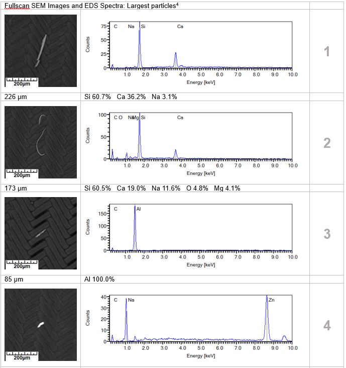
Excerpt from a laboratory SEM-EDS report: the largest particles on a filter with their BSE images and EDS spectra.
What elemental analysis adds
SEM-EDS particle analysis identifies what each particle found in an ISO 16232 / VDA 19.1 cleanliness test is made of and, from that composition, where it most likely came from. Our technical cleanliness testing laboratory in Monroe, Michigan runs the service on the Jomesa PSE scanning electron microscope. The work is ISO/IEC 17025:2017 accredited (PJLA) for SEM-EDS elemental analysis of automotive components.
An optical count on the Jomesa HFD tells you how many particles came off the part, how large they are, which are fibers, and which reflect light like metal. It does not tell you what they are made of. “Metallic shiny” is an optical estimate: a corroded steel chip may not shine, a shiny non-metal can be typed as metal, and light microscopy cannot separate hard particles from soft ones.
SEM-EDS (scanning electron microscopy with energy-dispersive X-ray spectroscopy, written SEM/EDX in ISO 16232 and VDA 19.1) closes that gap. The backscattered-electron (BSE) image brightens with atomic number, so metal stands out against the filter, with imaging to under 200 nm. The EDS detector reads each particle’s X-ray spectrum and reports the elements present, from boron (atomic number 5) to americium (atomic number 95). Software assigns a material class from that composition. That turns a count into an answer:
- Metallic, mineral, or organic: steel, aluminum, brass, and zinc read as metal by composition; quartz, corundum, and silicon carbide read as mineral; polymers and textile fibers read as organic.
- Machining chips, wear debris, or environmental: an iron-chromium chip points to stainless machining. An aluminum-oxide grain points to blasting or grinding media, quartz and silicate grains to casting sand or dust, and a fluorine-rich flake to a PTFE seal or coating.
- Hard or soft: abrasives such as corundum, silicon carbide, and quartz are identified by material, which is how a killer-particle question gets answered.
Composition links a contaminant to a likely source process. It does not name the source outright: that inference rests on the material class, the particle size, and the materials present in your process and its surroundings.
From count to identification
We were among the first worldwide to deploy the Jomesa PSE SEM-EDS scanning electron microscope that fully integrates with the Jomesa HFD. The HFD performs the ISO 16232 and VDA 19.1 particle count; the PSE identifies the particles it found. The filter stays on the same sample mount, so a particle located on the HFD is found again on the PSE without anyone searching for it by hand.
- The HFD scans the analysis filter and detects, sizes, and types every particle from 5 microns up as metallic shiny, non-metallic, or fiber.
- Lab staff flag the particles that need a material answer, one by one or by a rule, such as all metallic particles above a size limit.
- The filter mount moves to the PSE. The stage drives to each flagged position, captures the BSE image, acquires the EDS spectrum, and assigns a material class.
Fibers and organic particles have weak contrast under the electron beam, so they are measured optically and only the particles of interest go to the SEM.
When to order SEM-EDS
Under ISO 16232:2018 the standard analysis is gravimetry and the light-optical count, with SEM/EDX listed as an extended analysis. The revision of VDA 19.1 issued for comment in 2025 (the Yellow Print) adds a standard SEM/EDX analysis with uniform material classes. Add SEM-EDS particle analysis when the count alone will not settle the question:
- Contamination investigations: a field return or assembly problem points at particles, and you need to know what they are before you can say where they came from.
- Root cause on a failed Component Cleanliness Code: the material classes indicate where the excess came from. Machining chips from your own process, blasting or grinding media, casting sand, coating flakes, and packaging debris each read differently.
- Killer-particle questions: your specification, or your customer’s, limits hard or abrasive particles by material. Optical typification cannot verify that; elemental analysis can.
- Cleaning-process validation: compare material classes before and after a wash or deburr step to confirm the process removed the particles that matter, not only the easy ones. The precision cleaning and parts washing lines are on the same campus, so a process change can be re-tested in the same lab.
Your drawing or specification decides whether elemental analysis is required; if you are unsure, send the specification with your request. Contact the lab with your drawing and cleanliness specification to quote SEM-EDS with the count, or call +1 (734) 242-9935 or email sales@oemsupplier.com.
What the report contains
SEM-EDS particle analysis results are delivered in the same ISO 16232 / VDA 19.1 compliant report as the particle count for that test, with the BSE image, the EDS spectrum and the assigned material class for each analyzed particle. The elements on our accreditation scope are listed below; accreditation rules require any result outside that list to be identified on the report as outside the accredited scope. Tell us which document your specification cites, ISO 16232 or VDA 19.1, and its revision, so the report follows that notation.
Elements identified
The PJLA scope of accreditation (Accreditation No. 105574) lists SEM-EDS elemental analysis of automotive components. The SEM-EDS line names the method (Jomesa PSE manual and glass particle standard) and the technique (SEM EDS, Jomesa JMC3 microscope, PicEd software), quoted here as the certificate prints them. It lists 42 elements:
Al, As, B, Ba, Bi, Br, C, Ca, Cd, Cl, Co, Cr, Cu, F, Fe, Ga, Hf, Hg, I, In, K, Mg, Mn, Mo, N, Na, Nb, Ni, O, P, Pb, S, Sb, Se, Si, Sn, Ta, Ti, V, W and Zn, plus one entry the supplement prints as “Go”, which we have asked PJLA to confirm.
Elements outside that list can be detected and reported; accreditation rules require such results to be identified on the report as outside the accredited scope. The certificate and full scope are on the ISO/IEC 17025:2017 accreditation page.
Equipment
- Jomesa PSE scanning electron microscope with integrated EDS, the instrument the accreditation supplement lists as “Jomesa JMC3 microscope, PicEd software”
- Jomesa HFD (High Focal Depth) digital optical microscope as the optical front end that locates and sizes every particle first
- Glass particle standard for the SEM-EDS method, as named on the scope of accreditation
- Backscattered-electron imaging to under 200 nm; element detection from boron (Z=5) to americium (Z=95)
- PALL PCC61 and Gläser ACM18 ISO Class 5 extraction cabinets feed the same analysis filters

Frequently asked questions
Talk to an Expert – Get Answers Now.
Our specialists are ready to provide fast, reliable solutions tailored to your needs.